
[ad_1]
So the place will we flip for future scaling? We are going to proceed to look to the third dimension. We’ve created experimental units that stack atop one another, delivering logic that’s 30 to 50 p.c smaller. Crucially, the highest and backside units are of the 2 complementary sorts, NMOS and PMOS, which are the inspiration of all of the logic circuits of the final a number of a long time. We consider this 3D-stacked complementary metal-oxide semiconductor (CMOS), or CFET (complementary field-effect transistor), would be the key to extending Moore’s Regulation into the subsequent decade.
The Evolution of the Transistor
Steady innovation is an important underpinning of Moore’s Regulation, however every enchancment comes with trade-offs. To know these trade-offs and the way they’re main us inevitably towards 3D-stacked CMOS, you want a little bit of background on transistor operation.
Each metal-oxide-semiconductor field-effect transistor, or MOSFET, has the identical set of fundamental components: the gate stack, the channel area, the supply, and the drain. The supply and drain are chemically doped to make them each both wealthy in cell electrons (
n-type) or poor in them (p-type). The channel area has the other doping to the supply and drain.
Within the planar model in use in superior microprocessors as much as 2011, the MOSFET’s gate stack is located simply above the channel area and is designed to challenge an electrical area into the channel area. Making use of a big sufficient voltage to the gate (relative to the supply) creates a layer of cell cost carriers within the channel area that permits present to circulate between the supply and drain.
As we scaled down the basic planar transistors, what gadget physicists name short-channel results took middle stage. Principally, the space between the supply and drain turned so small that present would leak throughout the channel when it wasn’t presupposed to, as a result of the gate electrode struggled to deplete the channel of cost carriers. To deal with this, the business moved to a completely completely different transistor structure known as a
FinFET. It wrapped the gate across the channel on three sides to offer higher electrostatic management.
Intel introduced its FinFETs in 2011, on the 22-nanometer node, with the third-generation Core processor, and the gadget structure has been the workhorse of Moore’s Regulation ever since. With FinFETs, we may function at a decrease voltage and nonetheless have much less leakage, lowering energy consumption by some 50 p.c on the identical efficiency degree because the previous-generation planar structure. FinFETs additionally switched sooner, boosting efficiency by 37 p.c. And since conduction happens on each vertical sides of the “fin,” the gadget can drive extra present by way of a given space of silicon than can a planar gadget, which solely conducts alongside one floor.
Nonetheless, we did lose one thing in shifting to FinFETs. In planar units, the width of a transistor was outlined by lithography, and due to this fact it’s a extremely versatile parameter. However in FinFETs, the transistor width comes within the type of discrete increments—including one fin at a time–a attribute sometimes called fin quantization. As versatile because the FinFET could also be, fin quantization stays a big design constraint. The design guidelines round it and the will so as to add extra fins to spice up efficiency improve the general space of logic cells and complicate the stack of interconnects that flip particular person transistors into full logic circuits. It additionally will increase the transistor’s capacitance, thereby sapping a few of its switching pace. So, whereas the FinFET has served us effectively because the business’s workhorse, a brand new, extra refined strategy is required. And it’s that strategy that led us to the 3D transistors we’re introducing quickly.
 Within the RibbonFET, the gate wraps across the transistor channel area to reinforce management of cost carriers. The brand new construction additionally permits higher efficiency and extra refined optimization. Emily Cooper
This advance, the RibbonFET, is our first new transistor structure because the FinFET’s debut 11 years in the past. In it, the gate totally surrounds the channel, offering even tighter management of cost carriers inside channels that at the moment are shaped by nanometer-scale ribbons of silicon. With these nanoribbons (additionally known as
nanosheets), we are able to once more fluctuate the width of a transistor as wanted utilizing lithography.
With the quantization constraint eliminated, we are able to produce the appropriately sized width for the appliance. That lets us stability energy, efficiency, and value. What’s extra, with the ribbons stacked and working in parallel, the gadget can drive extra present, boosting efficiency with out rising the realm of the gadget.
We see RibbonFETs as the best choice for greater efficiency at cheap energy, and we will likely be introducing them in 2024 together with different improvements, corresponding to PowerVia, our model of
backside power delivery, with the Intel 20A fabrication course of.
Stacked CMOS
One commonality of planar, FinFET, and RibbonFET transistors is that all of them use CMOS expertise, which, as talked about, consists of n-type (NMOS) and p-type (PMOS) transistors. CMOS logic turned mainstream within the Nineteen Eighties as a result of it attracts considerably much less present than do the choice applied sciences, notably NMOS-only circuits. Much less present additionally led to better working frequencies and better transistor densities.
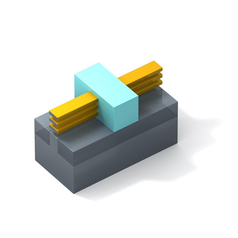
Up to now, all CMOS applied sciences place the usual NMOS and PMOS transistor pair aspect by aspect. However in a
keynote on the IEEE International Electron Devices Meeting (IEDM) in 2019, we launched the idea of a 3D-stacked transistor that locations the NMOS transistor on prime of the PMOS transistor. The next 12 months, at IEDM 2020, we offered the design for the first logic circuit using this 3D technique, an inverter. Mixed with applicable interconnects, the 3D-stacked CMOS strategy successfully cuts the inverter footprint in half, doubling the realm density and additional pushing the bounds of Moore’s Regulation.
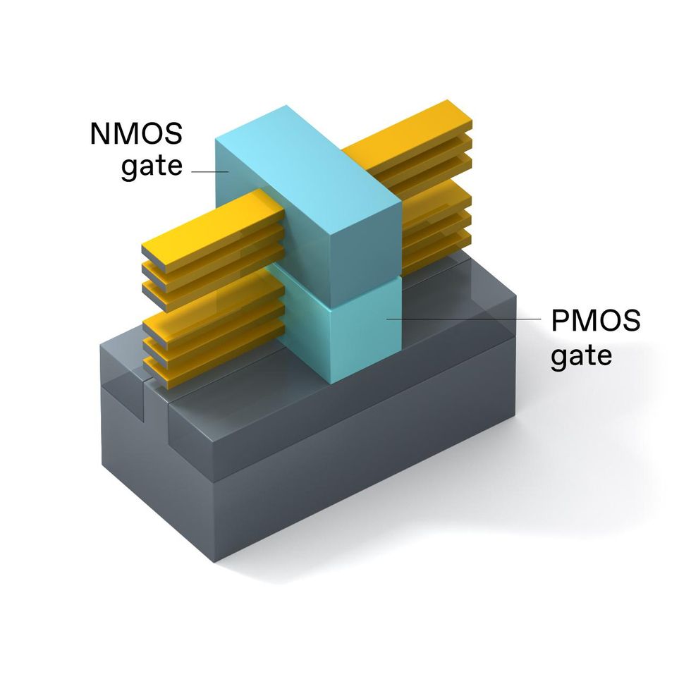 3D-stacked CMOS places a PMOS gadget on prime of an NMOS gadget in the identical footprint a single RibbonFET would occupy. The NMOS and PMOS gates use completely different metals.Emily Cooper
Benefiting from the potential advantages of 3D stacking means fixing quite a lot of course of integration challenges, a few of which is able to stretch the bounds of CMOS fabrication.
We constructed the 3D-stacked CMOS inverter utilizing what is named a self-aligned course of, during which each transistors are constructed in a single manufacturing step. This implies setting up each
n-type and p-type sources and drains by epitaxy—crystal deposition—and including completely different steel gates for the 2 transistors. By combining the source-drain and dual-metal-gate processes, we’re capable of create completely different conductive sorts of silicon nanoribbons (p-type and n-type) to make up the stacked CMOS transistor pairs. It additionally permits us to regulate the gadget’s threshold voltage—the voltage at which a transistor begins to modify—individually for the highest and backside nanoribbons.
How will we do all that? The self-aligned 3D CMOS fabrication begins with a silicon wafer. On this wafer, we deposit repeating layers of silicon and silicon germanium, a construction known as a superlattice. We then use lithographic patterning to chop away components of the superlattice and go away a finlike construction. The superlattice crystal supplies a robust assist construction for what comes later.
Subsequent, we deposit a block of “dummy” polycrystalline silicon atop the a part of the superlattice the place the gadget gates will go, defending them from the subsequent step within the process. That step, known as the vertically stacked twin supply/drain course of, grows phosphorous-doped silicon on each ends of the highest nanoribbons (the long run NMOS gadget) whereas additionally selectively rising boron-doped silicon germanium on the underside nanoribbons (the long run PMOS gadget). After this, we deposit dielectric across the sources and drains to electrically isolate them from each other. The latter step requires that we then polish the wafer right down to good flatness.
 An edge-on view of the 3D stacked inverter exhibits how difficult its connections are. Emily Cooper
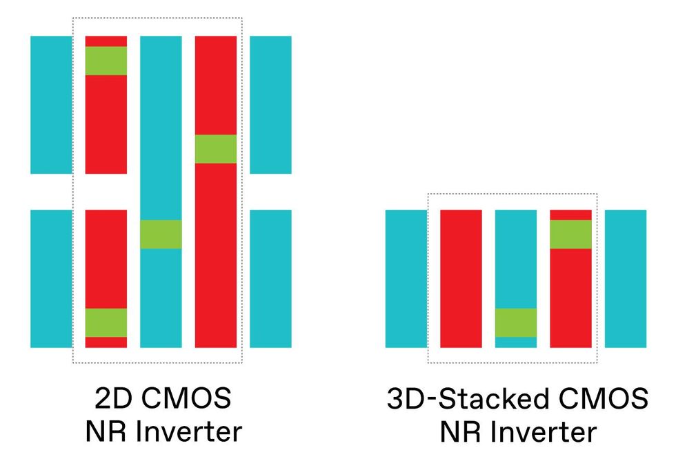 By stacking NMOS on prime of PMOS transistors, 3D stacking successfully doubles CMOS transistor density per sq. millimeter, although the actual density will depend on the complexity of the logic cell concerned. The inverter cells are proven from above indicating supply and drain interconnects [red], gate interconnects [blue], and vertical connections [green].
Lastly, we assemble the gate. First, we take away that dummy gate we’d put in place earlier, exposing the silicon nanoribbons. We subsequent etch away solely the silicon germanium, releasing a stack of parallel silicon nanoribbons, which would be the channel areas of the transistors. We then coat the nanoribbons on all sides with a vanishingly skinny layer of an insulator that has a excessive dielectric fixed. The nanoribbon channels are so small and positioned in such a means that we are able to’t successfully dope them chemically as we might with a planar transistor. As a substitute, we use a property of the steel gates known as the work perform to impart the identical impact. We encompass the underside nanoribbons with one steel to make a
p-doped channel and the highest ones with one other to type an n-doped channel. Thus, the gate stacks are completed off and the 2 transistors are full.
The method may appear complicated, however it’s higher than the choice—a expertise known as sequential 3D-stacked CMOS. With that technique, the NMOS units and the PMOS units are constructed on separate wafers, the 2 are bonded, and the PMOS layer is transferred to the NMOS wafer. As compared, the self-aligned 3D course of takes fewer manufacturing steps and retains a tighter rein on manufacturing value, one thing we demonstrated in analysis and reported at IEDM 2019.
Importantly, the self-aligned technique additionally circumvents the issue of misalignment that may happen when bonding two wafers. Nonetheless, sequential 3D stacking is being explored to facilitate integration of silicon with nonsilicon channel supplies, corresponding to germanium and III-V semiconductor supplies. These approaches and supplies could turn out to be related as we glance to tightly combine optoelectronics and different features on a single chip.
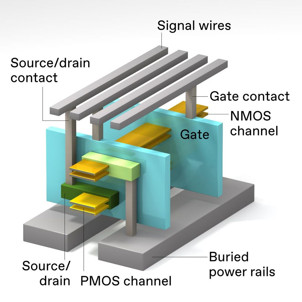 Making all of the wanted connections to 3D-stacked CMOS is a problem. Energy connections will should be made out of under the gadget stack. On this design, the NMOS gadget [top] and PMOS gadget [bottom] have separate supply/drain contacts, however each units have a gate in widespread.Emily Cooper
The brand new self-aligned CMOS course of, and the 3D-stacked CMOS it creates, work effectively and seem to have substantial room for additional miniaturization. At this early stage, that’s extremely encouraging. Gadgets having a gate size of 75 nm demonstrated each the low leakage that comes with wonderful gadget scalability and a excessive on-state present. One other promising signal: We’ve made wafers the place the smallest distance between two units of stacked units is just
55 nm. Whereas the gadget efficiency outcomes we achieved are usually not information in and of themselves, they do examine effectively with particular person nonstacked management units constructed on the identical wafer with the identical processing.
In parallel with the method integration and experimental work, we’ve got many ongoing theoretical, simulation, and design research underway seeking to present perception into how finest to make use of 3D CMOS. By means of these, we’ve discovered among the key issues within the design of our transistors. Notably, we now know that we have to optimize the vertical spacing between the NMOS and PMOS—if it’s too quick it’ll improve parasitic capacitance, and if it’s too lengthy it’ll improve the resistance of the interconnects between the 2 units. Both excessive ends in slower circuits that devour extra energy.
Many design research, corresponding to one by
TEL Research Center America presented at IEDM 2021, concentrate on offering all the required interconnects within the 3D CMOS’s restricted area and doing so with out considerably rising the realm of the logic cells they make up. The TEL analysis confirmed that there are lots of alternatives for innovation find the most effective interconnect choices. That analysis additionally highlights that 3D-stacked CMOS might want to have interconnects each above and under the units. This scheme, known as buried power rails, takes the interconnects that present energy to logic cells however don’t carry information and removes them to the silicon under the transistors. Intel’s PowerVIA expertise, which does simply that and is scheduled for introduction in 2024, will due to this fact play a key function in making 3D-stacked CMOS a industrial actuality.
The Way forward for Moore’s Regulation
With RibbonFETs and 3D CMOS, we’ve got a transparent path to increase Moore’s Regulation past 2024. In a 2005 interview during which he was requested to mirror on what turned his legislation, Gordon Moore admitted to being “periodically amazed at how we’re capable of make progress. A number of instances alongside the best way, I assumed we reached the top of the road, issues taper off, and our inventive engineers give you methods round them.”
With the transfer to FinFETs, the following optimizations, and now the event of RibbonFETs and ultimately 3D-stacked CMOS, supported by the myriad packaging enhancements round them, we’d prefer to suppose Mr. Moore will likely be amazed but once more.
From Your Website Articles
Associated Articles Across the Internet
Source link