Paul Eisle invented the primary PCB in 1936. Nevertheless, it became popular only inside the 1950s when the US armed service started using the technology with bomb detonators. Today, PCB Circuit Boards are vital to almost all equipment, including cars, mobile phones, computers, etc. Get the Best information about PCB.
Table of Contents
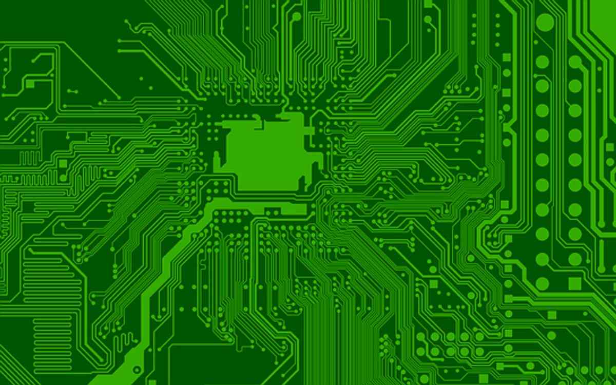
How Is A Printed Rounds Board Manufactured?
To make a custom-made PCB, first, the digital diagram of the required routine is prepared using a Personal computer Aided Design (CAD) application. After that, the original PCB was developed using Personal computer Aided Manufacturing Software technological innovation.
The common materials used for PCBs are FR4, FR4 High Temperature, Polyimide, GeTek, Rogers, Arlon, Nelco, Alumina, Fine ceramic, Bakelite, FR1, CEM1, and also CEM5. The size and fullness of the board depend upon the circuit’s necessities. First, the essence is coated with a level of copper.
Then, the standard diagram is printed around the board using the photosensitive coating. Finally, the undesired birdwatcher is etched out from the table to form copper “tracks,” named traces. This process is known as Photoengraving.
There are two other frequent methods used for developing joining atoms. First, PCB milling is often a mechanical system where nuisance copper is removed having CNC machines. Another practice is Silk-Screen printing, everywhere special ink that is etch-resistant is used to cover the areas where the copper traces have to be manufactured.
Once the board is completely ready with copper traces, cracks are drilled into the motherboard to assemble leaded electrical and electronic components. Forgoing, special Tungsten Carbide tool bits or laser is needed. The holes are made with hollow rivets and coated through an electroplating process, thus forming a stainless steel connection among the various coatings.
The next step is covering the entire board, except holes in addition to pads, with masking content. Materials commonly used for this purpose usually are: lead solder, lead-free of charge solder, OSP (Entek), deep/hard gold (electrolytic nickel gold), immersion gold (electroless Pennie gold – ENIG), line bondable gold (99. 00% pure gold), immersion magic, flash gold, immersion jar (white tin), carbon tattoo, and SN 100CL, an excellent alloy of tin, birdwatcher, and nickel. The last phase is screen-printing, where the tale and text are published on the PCB.
Testing Regarding PCB
Before assembly regarding components or delivery regarding Printed Circuit Boards, the particular board should be tested to locate any possible “shorts” and “opens” that could lead to any nonfunctioning board. A “short” indicates an unwanted connection, and an “open” means that two points that should have been connected are unconnected.
All such errors ought to be fixed before PCB is set up. It is important to note that not all PCB Manufacturing shops test the actual boards before shipping. It is sometimes considered an added price but vital to give a fully functioning board before adding components.
PCB Set up
Once the board is prepared, components are assembled and added to the surface as per the signal diagram. Some of the standard setup techniques used are surface-mount construction and through-hole building. Sometimes, a combination of these two methods is also used for assembly.
Varieties of Printed Circuit Boards
One-Sided Board
This is a minor complex of the Printed Outlet Boards since there is only one substrate layer. As a result, most electrical parts and ingredients are fixed on one area, and copper traces have the other side.
Double On the sides Board
This is the most common board, where parts and components are attached to both sides of the substrate. In such cases, double-sided PCBs with connecting remnants on both sides are used. Double-sided Printed Circuit Boards generally use through-hole construction for the assembly of components.
Multiple Layered Board
Multi-split PCB consists of several levels of substrate separated through insulation. The most common multilayer panels are four, six, eight, and ten layers. However, the total number of layers produced can exceed over forty-two layers. These types of boards are utilised in highly complex electric circuits.
Read Also: An Easy Introduction To The World Of Smartphone In Addition To IPhone Spy Software